Hardware
This page lists and describes the hardware found inside the Nintendo 3DS. Many of these parts are custom made and are expanded upon here or in other pages.
Specifications
| Type | Name | Datasheet | Source |
|---|---|---|---|
| SoC | Nintendo 1048 0H (Custom): CPU, GPU, VRAM & DSP all on one chip. | N/A | N/A |
| ARM11 Processor Core | ARM11 MPCore 2x 268MHz(~268123480 Hz) & 2x VFP Co-Processor | [1] | [11] |
| ARM9 Processor Core | ARM946 134MHz(~134058675 Hz) | [2] | |
| GPU | DMP PICA 268MHz | N/A | [11] |
| DSP | CEVA TeakLite. Based on Atmel AT75C. 134Mhz. 24ch 32728Hz sampling rates. | N/A | [11] [3] |
| VRAM | 6 MB within SoC. Independent of system memory (FCRAM). | N/A | [11] |
| FCRAM | 2x64MB Fujitsu MB82M8080-07L | [4][5][6] | [5] |
| Storage | Toshiba THGBM2G3P1FBAI8 1GB NAND Flash | N/A | N/A |
| Power Management | Texas Instruments PAIC3010B 0AA37DW | N/A | FCC filing |
| Gyroscope | Invensense ITG-3270 MEMS Gyroscope | [7] | N/A |
| Accelerometer | ST Micro 2048 33DH X1MAQ Accelerometer Model LIS331DH | [8] | N/A |
| Wifi | 802.11b/g Atheros AR6014 | [9] | N/A |
| Infrared IC | NXP infrared IC, "S750 0803 TSD031C" | [12] | [10] |
| Auxiliary Microcontroller | Renesas Electronics UC CTR, custom Nintendo microcontroller | N/A | N/A |
| ? | "TI 93045A4 OAAH86W" | N/A | N/A |
- [11] Official Documentation
- [5],[10] According to iFixit.com (source):
- Datasheet for memory is for a chip in the same series, it has less memory than the one inside the 3DS (128mbits vs 512mbits).
- There is a trove of data on the FCC website at [10].
- [12] This IC is somewhat similar to this.
New_3DS Specifications
| Type | Description | Datasheet | Source |
|---|---|---|---|
| ARM11 Processor Core | ARM11 MPCore 4x 268MHz(?) & 4x VFP Co-Processor | [11] | |
| FCRAM | 256MB | ||
| VRAM | 6 MB within SoC. Independent of system memory (FCRAM). | N/A | |
| 4MB of additional memory. | N/A | ||
| NFC | |||
| MVD |
Note that 4 cores is also the maximum number of cores available with ARM11-MPCore.
FCRAM
There is one FCRAM (Fast Cycle RAM) IC in the 3DS, produced by Fujitsu and branded as MB82M8080-07L. The Fujitsu MB82M8080-07L chip internally contains 2 dies, where each die is branded MB81EDS516545 and MB82DBS08645.
The MB81EDS516545 die is a CMOS Fast Cycle Random Access Memory (FCRAM) with Low Power Double Data Rate (LPDDR) SDRAM Interface containing 512MBit storage accessible in a 64-bit format. The MB81EDS516545 is suited for consumer applications requiring high data bandwidth with low power consumption.
SoC
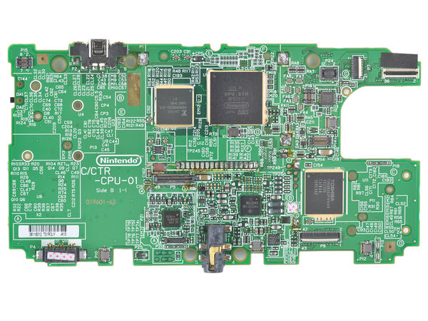
The 3DS has much of it's internals housed in a SoC (System on Chip) just like it's predecessors. This is done to reduce build costs, cut down on power consumption, as well as make the PCB layout less complex and make the system harder to tamper with. The SoC, branded as the Nintendo 1048 0H, contains the CPU, GPU, DSP and VRAM.
According to official documents, the CPU used is a dual-core ARM11 CPU, clocked at 268MHz. One core is dedicated to system software, while the other is used for application programming, each known as the syscore and appcore, respectively.
GPU
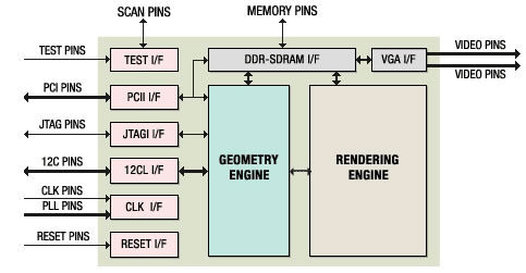
As mentioned, DMP's (Digital Media Proffesionals) PICA 200, 268Mhz. This GPU supports OpenGL ES 1.1.
Block diagram of an ULTRAY2000 based architecture PICA200
Images
Front
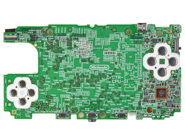
Back
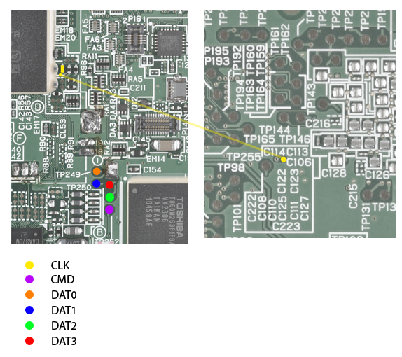
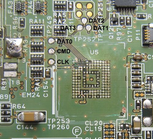
NAND pinout
NAND dumping has been successful, but the image is encrypted.
Normal model
XL model
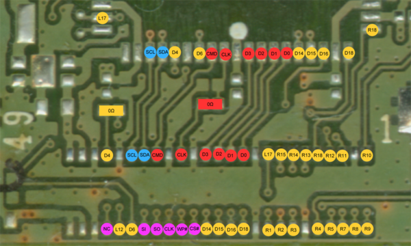
WiFi dongle pinout
SDIO interface is colored red:
- CLK
- CMD
- D0, D1, D2, D3
This is the interface for the 'NEW' WiFi module (based on Atheros AR6002) first included in DSi.
The proprietary and by now ancient DS-mode WiFi is colored yellow, pins are unknown.
I2C eeprom is colored blue:
- SCL
- SDA
SPI Flash is colored purple:
- CLK
- CS#
- SI
- SO
- WP#
- NC
Auxiliary Microntroller
Monitors HOME button, WiFi switch, 3D slider, volume control slider. Controls LEDs, various power supplies.
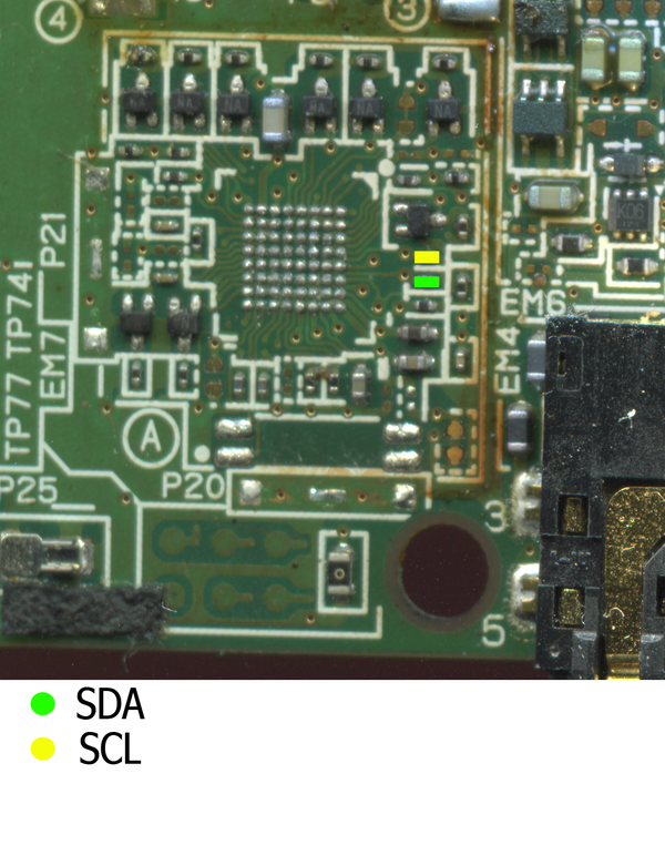
Devices attached to I2C bus:
- UC (master?)
- Accelerometer (slave address 0x18)
- SoC (master? slave?)
